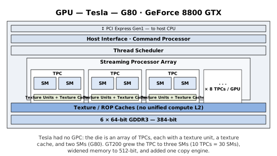
Every CUDA-capable GPU, from the 2006 G80 that launched the platform to today’s Blackwell parts, is assembled from the same handful of ingredients: a host interface to the PCI Express bus, a front-end that distributes work, one or more copy engines, an on-chip last-level cache, a DRAM interface, and an array of Streaming Multiprocessors (SMs) grouped into clusters. What changes across the generations is the scale of each ingredient and the degree of specialization within the SM. This section walks that evolution twice—first at the level of the whole GPU (Section 2.6.1), then inside the SM itself (Section 2.6.2)—and closes with the programmable GPU-scale locality that Hopper introduced (Section 2.6.3).
The generations, each named for a physicist and first shipped in a flagship ASIC, are summarized in Table 2-1.
| Architecture | Year | First silicon | SM | What it introduced |
|---|---|---|---|---|
| Tesla | 2006 | G80 | 1.0 | The first CUDA hardware; double precision arrived with GT200 (SM 1.3, 2008) |
| Fermi | 2010 | GF100 | 2.0 | The first unified cache hierarchy and full-throughput integer math |
| Kepler | 2012 | GK104 | 3.0 | The wide, power-efficient “SMX”; the compute GK110/GK210 followed |
| Maxwell | 2014 | GM204 | 5.2 | A partitioned SM built for performance-per-watt |
| Pascal | 2016 | GP100 | 6.0 | NVLink, HBM2, and the return of the TPC |
| Volta | 2017 | GV100 | 7.0 | The first Tensor Cores and a separate integer datapath |
| Turing | 2018 | TU102 | 7.5 | Second-generation Tensor Cores and the first RT Cores |
| Ampere | 2020 | GA100 / GA102 | 8.0 / 8.6 | Doubled FP32 throughput and a very large L2 |
| Ada Lovelace | 2022 | AD102 | 8.9 | Consumer contemporary of Hopper; SM follows Ampere’s GA10x, so it is not diagrammed separately |
| Hopper | 2022 | GH100 | 9.0 | FP8 Tensor Cores, the Tensor Memory Accelerator, and thread-block clusters |
| Blackwell | 2025 | GB202 / GB200 | 12.0 / 10.0 | FP4 Tensor Cores; INT32 folded back into the FP32 lanes |
Table 2-1. The CUDA-capable GPU generations, from the platform’s launch to the present.
The nomenclature is worth a word: names like GF100 and GK104 refer to the ASIC that implements the GPU, with the second letter identifying the architecture (Fermi, Kepler, and so on). NVIDIA also uses several of the architecture names—Tesla most confusingly—as product brands for its datacenter boards. To keep the two apart, this book uses “Tesla-class hardware,” “Fermi-class hardware,” and the like for the architectural families.
CUDA’s simplified view of the GPU (Figure 2-32 shows the earliest example) includes:
The architectural papers cited at the end of this chapter give a more complete picture, including graphics-specific functionality such as antialiased rendering.
The host interface—sometimes called the command processor—reads the stream of GPU commands the CPU submits over PCI Express (memcpy and kernel launch commands, among others) and dispatches each to the appropriate hardware: kernel launches go to the GigaThread engine, which distributes their thread blocks across the SMs, and copies go to the copy engines. It also implements synchronization between the CPU and GPU, between engines on a GPU, and between GPUs; in CUDA, that functionality is exposed primarily through the Stream and Event APIs (Chapter 6). The host interface has been updated to stay current with the PCI Express standard, from Gen1 on G80 to Gen5 on Hopper and Blackwell, each generation roughly doubling host↔︎device bandwidth (Section 2.7).
Copy engines perform host↔︎device transfers while the SMs compute. The earliest CUDA hardware had none (the G80 could not overlap copy with kernel execution at all); GT200 added one; and Fermi-class Tesla boards added a second, so that transfers in both directions could overlap a running kernel. Datacenter parts have exposed two or more ever since, while GeForce parts historically exposed one and now report several. The copy engines are designed to saturate the GPU’s NVLink or PCI Express interconnects, and can do layout conversions such as converting between CUDA arrays and linear memory at line rates.
One of the quieter revolutions in the GPU is the last-level cache. Tesla-class hardware had no general-purpose L2 at all—only small texture and raster caches—so every uncoalesced or reused access went to DRAM. Fermi introduced a modest 768 KB write-through L2 shared by the whole chip—the arbiter of all external memory traffic to and from the GPU, and the unit in which the GPU implements hardware support for global-memory atomics. It has grown relentlessly since: 2 MB on Maxwell, 4–6 MB through Pascal and Volta, and then a step change to 40 MB on the A100, 50 MB on Hopper, and 96–128 MB on Blackwell. A cache this large changes how kernels behave—working sets that once thrashed DRAM now live on chip—and it is a major reason modern GPUs sustain their throughput despite memory systems that have grown far more slowly than their arithmetic.
For many applications, the L2 does not serve to reduce latency so much as to aggregate bandwidth to the HBM, translating requests from the SMs and other clients of the memory subsystem into reasonable-looking memory transactions for the various memory controllers across the chip. In fact, starting with Fermi, a hash function was introduced to make it difficult or impossible to steer memory operations onto any particular memory controller.
That hash addressed a real pathology of the earlier hardware, known as partition camping. Device memory is striped across the partitions in contiguous runs—256 bytes at a time on the Tesla-generation parts—so a fixed field of the physical address selected which partition, and therefore which memory controller, a given transaction reached. When the thread blocks running concurrently all touched addresses separated by a multiple of the stripe span, their traffic piled onto a subset of the partitions while the rest sat idle, and effective bandwidth collapsed to that fraction of the memory system. Partition camping was the global-memory analog of a shared-memory bank conflict—not a collision among the threads of a warp, but a collision among the blocks resident on the machine.
The canonical victim was matrix transpose, whose concurrently active blocks touch tiles separated in memory by a full row of the matrix; for unfortunate dimensions, every one of them could land on the same partition. NVIDIA’s whitepaper Optimizing Matrix Transpose in CUDA worked around it by numbering the thread blocks along diagonals, scattering their tiles across the partitions by hand. Address hashing retired the technique: by scrambling the bits that select the partition, it keeps regularly strided accesses from converging on one controller, so partition camping is no longer something a kernel must be designed to avoid. The distribution of memory traffic across controllers is now left entirely to the hardware.
It is worth being precise about what type of memory may be cached by the L2. The GPU’s own device (HBM) memory always can be cached for reuse, but whether host (CPU) memory may be cached depends on the type of interconnect. PCI Express is not a coherency link at all: coherence across it is handled in software, through page faults, so host memory reached over PCIe is never hardware-cached by the GPU.
A coherent NVLink connection, such as between the CPU and GPU on the Grace Hopper and Grace Blackwell superchips, gives the CPU and GPU a single shared address space with hardware-maintained coherence (Section 2.7); even so, the caching is asymmetric, because the CPU can cache the GPU’s memory while the GPU’s accesses to CPU memory are not cached.
The GPU-wide DRAM interface coalesces memory requests and, on modern hardware, feeds an appetite for bandwidth that dwarfs any CPU’s. The earliest (SM 1.x) hardware had onerous coalescing rules—addresses had to be contiguous and aligned—but from SM 1.2 (GT200) onward, accesses could be coalesced by locality regardless of alignment, and Fermi’s L2 made reuse cheap. The memory technology itself has moved from GDDR3 on G80 (about 86 GB/s) through successive GDDR generations on consumer parts to stacked HBM on datacenter parts beginning with Pascal’s HBM2, reaching multiple terabytes per second on Hopper and Blackwell.
Beginning with Pascal’s GP100, datacenter GPUs gained NVLink, a proprietary interconnect for GPU↔︎GPU (and later CPU↔︎GPU) traffic far faster than PCI Express. Its aggregate bandwidth has doubled almost every generation—160 GB/s on P100, 300 on V100, 600 on A100, 900 on H100, and 1.8 TB/s on the Blackwell B200—and Hopper added an external NVLink Switch to extend it across many GPUs. NVLink is covered in detail in Section 2.7; on consumer parts it appeared only briefly (Turing and the RTX 3090) and has since been dropped. The GPU-level figures below show where the NVLink ports attach.
Between the whole GPU and the individual SM sits an intermediate grouping. Tesla-class hardware had no GPC: its die was a Streaming Processor Array of Texture Processing Clusters (TPCs), each bundling a texture unit, a texture cache, and two or three SMs (Figure 2-32). Fermi introduced the Graphics Processing Cluster (GPC)—a raster engine plus several SMs, with texture pulled down into each SM—and Pascal brought the TPC back inside the GPC as a two-SM unit, the arrangement used ever since. For most of CUDA’s history, these boundaries were invisible to software; that changed with Hopper (Section 2.6.3).
The figures that follow trace this whole-GPU organization across the generations. Notice how little the top-level recipe changes even as the SM count climbs from 16 to nearly 200, the L2 grows by two orders of magnitude, and HBM and NVLink appear.
Figure 2-32. Tesla GPU (G80): a Streaming Processor Array of TPCs, each with a texture cache and two SMs; no GPC, and no unified compute L2.
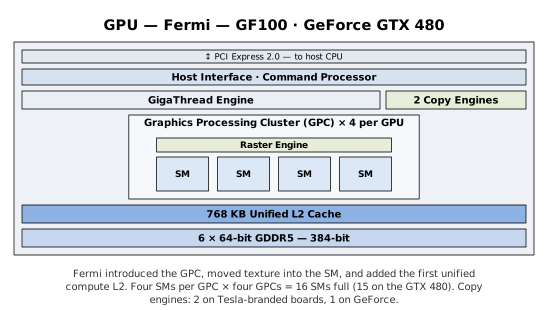
Figure 2-33. Fermi GPU (GF100): the GPC debuts, texture moves into the SM, and the first unified compute L2 appears.
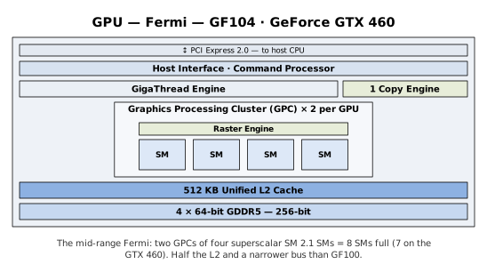
Figure 2-34. Fermi GPU (GF104): the mid-range part, two GPCs of superscalar SM 2.1 cores.
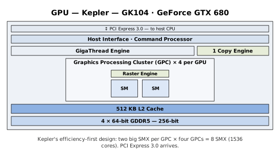
Figure 2-35. Kepler GPU (GK104): two wide “SMX” per GPC; PCI Express 3.0 arrives.
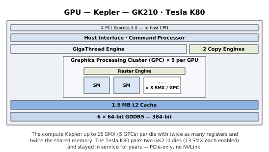
Figure 2-36. Kepler GPU (GK210): the compute Kepler with twice as many registers and twice the shared memory, shipped in the long-lived, PCIe-only Tesla K80.
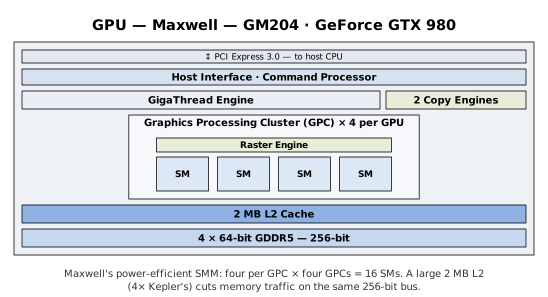
Figure 2-37. Maxwell GPU (GM204): power-efficient SMMs backed by a large 2 MB L2 cache.
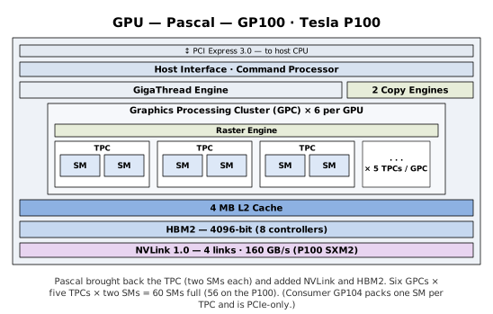
Figure 2-38. Pascal GPU (GP100): TPCs return inside the GPC; NVLink and HBM2 arrive.
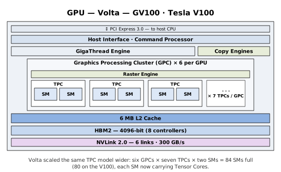
Figure 2-39. Volta GPU (GV100): the same hierarchy scaled to 84 SMs, each now carrying Tensor Cores.
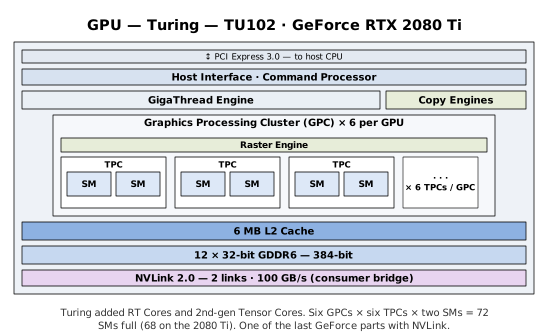
Figure 2-40. Turing GPU (TU102): RT Cores arrive; one of the last GeForce parts with NVLink.
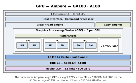
Figure 2-41. Ampere GPU (GA100): a 40 MB partitioned L2 and a 5120-bit HBM2e interface feed 108 SMs.
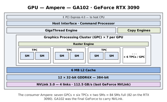
Figure 2-42. Ampere GPU (GA102): the consumer part, and the final GeForce to carry NVLink.
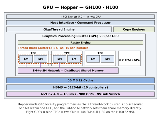
Figure 2-43. Hopper GPU (GH100): thread-block clusters make GPC locality programmable through the SM-to-SM distributed-shared-memory network (Section 2.6.3).
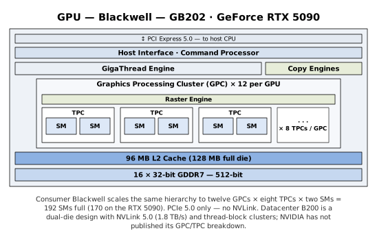
Figure 2-44. Blackwell GPU (GB202): 192 SMs across twelve GPCs, PCIe-only. The datacenter B200 is a dual-die design with NVLink 5.0 and thread-block clusters, whose GPC/TPC breakdown NVIDIA has not published.
The workhorse of the GPU is the Streaming Multiprocessor. Every SM, in every generation, is built from the same parts: one or more warp schedulers that issue instructions from resident warps; a register file; execution units—lanes for single-precision floating point and integer arithmetic, and Special Function Units (SFUs) for transcendental approximations; shared memory for intra-block data exchange; and read-only constant (and, on early hardware, texture) caches. What the generations add is more lanes, more kinds of lanes, and a steadily richer memory hierarchy inside the SM.
The Tesla SM (Figure 2-45) is the elemental version:
eight Streaming Processors (SPs) fed by a single warp scheduler, two
SFUs, and—starting with GT200—a single double-precision unit, over a
shared register file and 16 KB of shared memory. Load/store traffic and
texture were handled by the enclosing TPC, not the SM. Tesla-class
hardware paid dearly for uncoalesced memory access (up to 6× on early
parts, ~2× from GT200) and had only a 24-bit integer multiplier, so
performance-critical code used the __mul24() intrinsic;
full 32-bit multiplication was emulated.
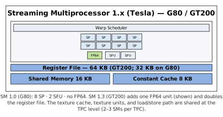
Figure 2-45. Streaming Multiprocessor 1.x (Tesla).
Fermi (Figures 2-46 and 2-47) reorganized the SM
into execution blocks of 16 cores—two blocks (32 cores) on GF100’s SM
2.0, three (48 cores) on GF104’s superscalar SM 2.1—fed by dual warp
schedulers over a shared 128 KB register file. Fermi added a full 32-bit
integer multiplier (making __mul24() a pessimization),
first-class double precision, load/store units, surface load/store, and
a configurable 64 KB pool split between L1 cache and shared memory. It
was also the first SM to cache texture within the SM itself.
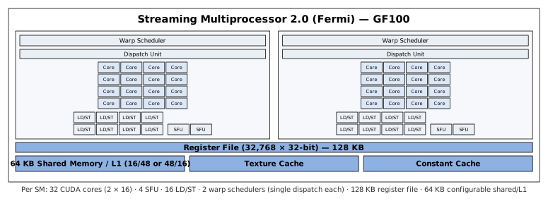
Figure 2-46. Streaming Multiprocessor 2.0 (Fermi, GF100).
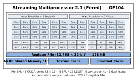
Figure 2-47. Streaming Multiprocessor 2.1 (Fermi, GF104): three core blocks fed by two dual-issue schedulers.
Kepler’s “SMX” (Figures 2-48 and 2-49) was a departure: 192 cores, four dual-issue warp schedulers, and a 256 KB register file, all clocked lower for efficiency and paired with a 48 KB read-only/texture cache. GK110 raised double-precision throughput for compute; GK210—shipped in the Tesla K80—carried twice as many registers (512 KB) and twice the shared memory (128 KB), which kept it viable for years after its successors arrived.
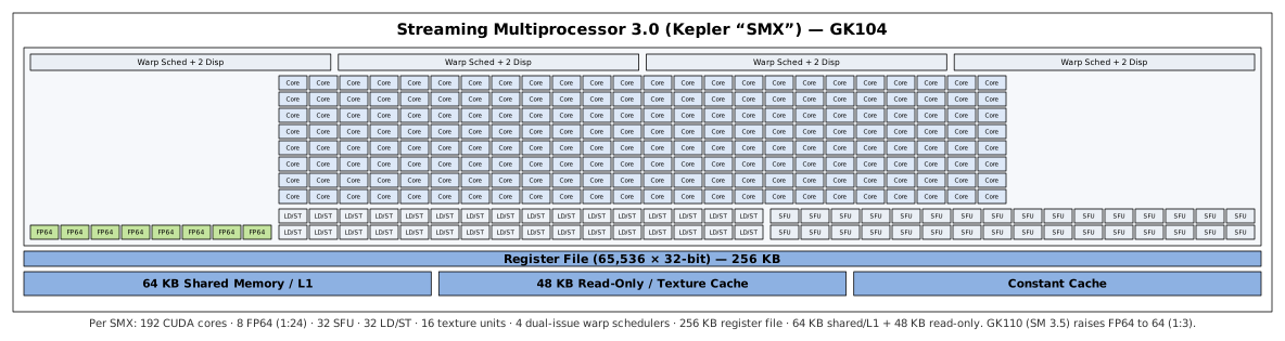
Figure 2-48. Streaming Multiprocessor 3.0 (Kepler “SMX,” GK104).
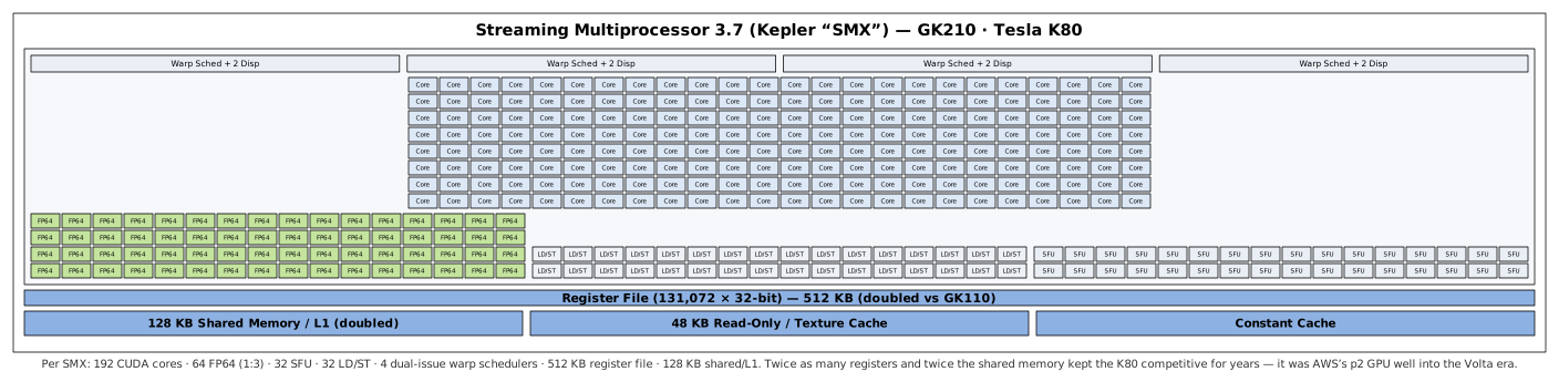
Figure 2-49. Streaming Multiprocessor 3.7 (Kepler, GK210): the doubled register file and shared memory of the Tesla K80.
Maxwell (Figure 2-50) made the partitioning explicit: four processing blocks of 32 cores, each with its own warp scheduler and—crucially—its own 64 KB register file. The register file, once a single array shared across the SM, was now split into four per-partition banks—an arrangement every later generation inherits. Maxwell also pulled shared memory back out into a dedicated 96 KB block, separate from the L1/texture cache.
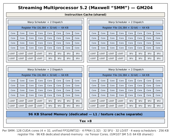
Figure 2-50. Streaming Multiprocessor 5.2 (Maxwell “SMM,” GM204).
Pascal’s GP100 SM (Figure 2-51) kept the partitioned design but at two blocks of 32, and restored high double-precision throughput (one FP64 lane for every two FP32) for HPC. The consumer GP104 instead used four blocks with minimal FP64—the first of many splits between compute-oriented and graphics-oriented SMs within a generation.
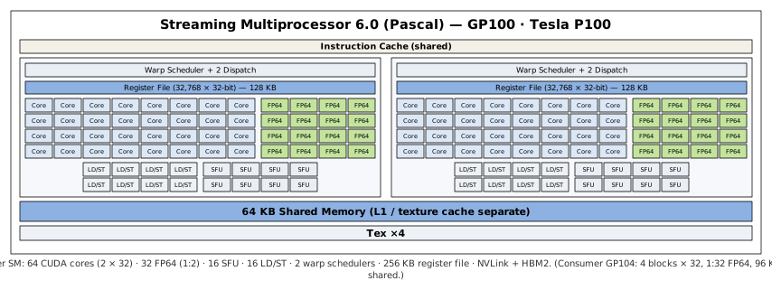
Figure 2-51. Streaming Multiprocessor 6.0 (Pascal, GP100).
Volta’s GV100 SM (Figure 2-52) is the template every subsequent generation follows. Its four partitions each gained an L0 instruction cache beneath the shared L1, a separate INT32 datapath so integer and floating-point instructions can issue together, and—most consequentially—two Tensor Cores, the matrix-multiply units that would reshape the platform. The 128 KB unified L1/shared pool replaced Fermi’s fixed split with a configurable carveout.
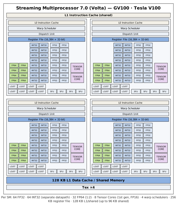
Figure 2-52. Streaming Multiprocessor 7.0 (Volta, GV100): first Tensor Cores, separate INT32 datapath, per-partition L0 instruction cache.
Turing (Figure 2-53) brought second-generation Tensor Cores (adding INT8 and INT4) and the first RT Core for ray tracing, at the cost of the compute-class double-precision throughput that stayed on the datacenter line.
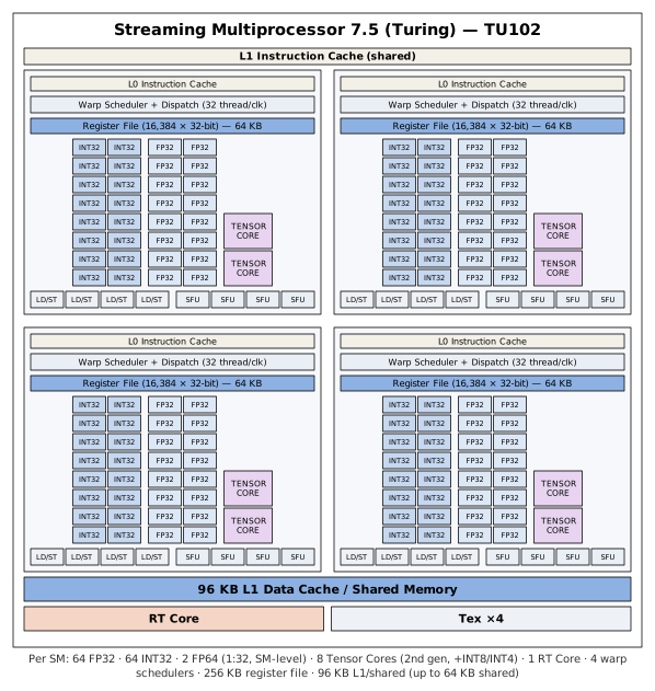
Figure 2-53. Streaming Multiprocessor 7.5 (Turing, TU102): 2nd-generation Tensor Cores and an RT Core.
Ampere widened the arithmetic in a way worth understanding precisely. The datacenter GA100 (Figure 2-54) kept Volta’s separate 64 FP32 + 64 INT32 lanes and added third-generation Tensor Cores with TF32 and structured sparsity. The consumer GA102 (Figure 2-55) instead made one of each partition’s two datapaths capable of FP32 or INT32, doubling peak FP32 to 128 lanes per SM—the single biggest reason Ampere’s graphics throughput jumped over Turing’s. (Ada Lovelace, the 2022 consumer line, refines this same SM with newer Tensor and RT Cores.)
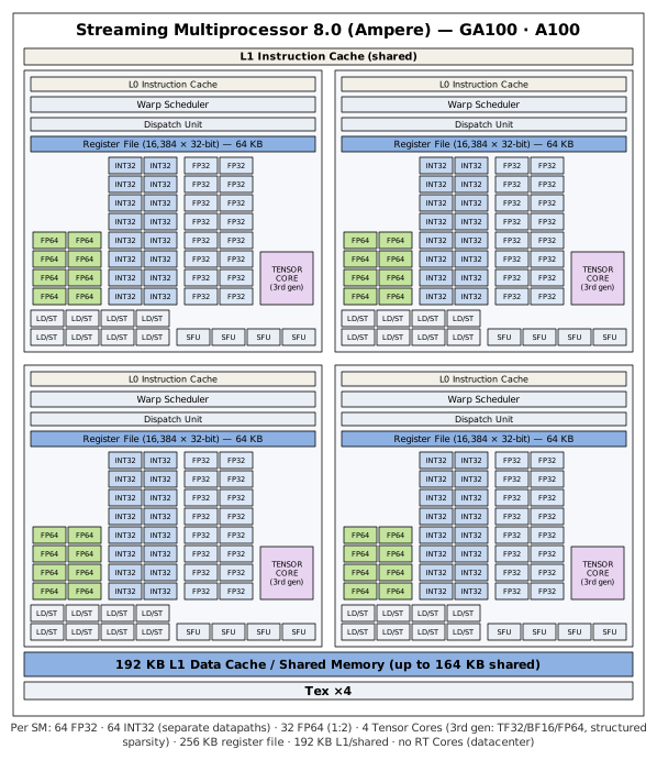
Figure 2-54. Streaming Multiprocessor 8.0 (Ampere, GA100): separate INT32, 3rd-generation Tensor Cores, 192 KB L1/shared.
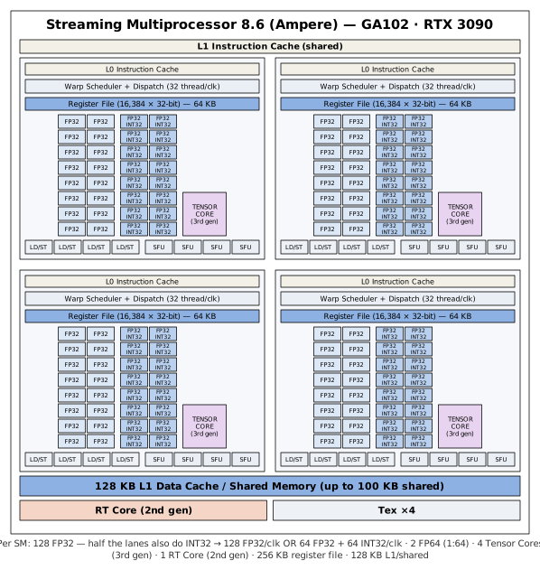
Figure 2-55. Streaming Multiprocessor 8.6 (Ampere, GA102): the shared FP32/INT32 datapath that doubles FP32 throughput.
Hopper’s GH100 SM (Figure 2-56) combined the widened FP32/INT32 datapaths with a dedicated FP64 datapath (restoring 1:2 double precision), fourth-generation Tensor Cores with FP8 and a Transformer Engine, and a 256 KB L1/shared pool. It also added the Tensor Memory Accelerator (TMA), an asynchronous engine that bulk-copies tiles between global and shared memory, freeing the SM’s threads from address arithmetic.
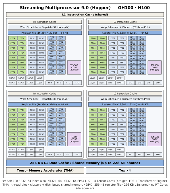
Figure 2-56. Streaming Multiprocessor 9.0 (Hopper, GH100): FP8 Tensor Cores, dedicated FP64, and the Tensor Memory Accelerator.
Blackwell’s consumer GB202 SM (Figure 2-57) folds INT32 fully back into the 128 FP32 lanes—every core does floating point or integer—and carries fifth-generation Tensor Cores with FP4 and a second-generation Transformer Engine. The datacenter B200 adds high-throughput FP64 and a dedicated on-SM Tensor Memory, and pairs two such dies as a single CUDA device.
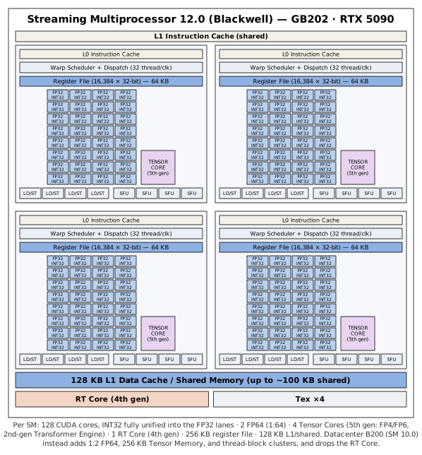
Figure 2-57. Streaming Multiprocessor 12.0 (Blackwell, GB202): unified FP32/INT32 lanes and 5th-generation (FP4) Tensor Cores.
It is worth pausing to take in the sweep of this evolution. The G80 that introduced CUDA in 2006 packed 681 million transistors into 480 mm² of silicon; the GB202 at the heart of the 2025 GeForce RTX 5090 packs 92.2 billion into 750 mm²—roughly 135 times as many—and the datacenter Blackwell B200, built from two dies that present themselves to CUDA as a single GPU, comes to 208 billion. In less than two decades, the transistor budget of a flagship GPU grew by more than two orders of magnitude.
And yet, set the Tesla and Blackwell Streaming Multiprocessor diagrams side by side and the family resemblance is unmistakable. An SM is still, at bottom, one or more warp schedulers feeding a register file and a bank of SIMD lanes, backed by a pool of shared memory and a few special-function units. The lanes have multiplied and specialized—double-precision units, dedicated integer pipelines, Tensor Cores, an L0 instruction cache in each partition—and the register file that was once shared across the SM was split into per-partition banks with Maxwell. But the shape of the machine, and the programming model that rides on it—warps of 32 threads, shared memory, occupancy—has proven remarkably durable. Much of what a programmer learned about the G80 still applies to a GPU with a hundred times the transistors; the newer hardware mostly asks that those lessons be applied at greater scale, and that its new specialized units be kept fed.
For most of CUDA’s history, the GPC and TPC boundaries of Section 2.6.1 were invisible to software: the block scheduler placed thread blocks opaquely, and there was no way to reason about which SMs shared a GPC. Hopper (SM 9.0) changed that by making GPC-level locality programmable, through thread-block clusters.
A cluster is a group of thread blocks—up to 8 portably, or 16 on
hardware that opts in—that the runtime guarantees to co-schedule on SMs
within a single GPC. That co-residency is what makes the new
capability possible: an SM-to-SM network inside the GPC lets the blocks
in a cluster read, write, and perform atomics on one another’s shared
memory directly, without a round trip through L2 or global memory.
NVIDIA calls this aggregate address space distributed shared
memory (DSMEM), and reports block-to-block exchange several
times faster than the global-memory path it replaces. Clusters are
launched with cudaLaunchKernelEx (or the
__cluster_dims__ qualifier) and coordinated through the
cluster tier of cooperative groups—cluster.sync(), cluster
barriers, and shared-memory address mapping across blocks.
The Hopper and Blackwell GPU figures (Figures 2-43 and 2-44) show a cluster spanning several SMs within one GPC, connected by this SM-to-SM network. The feature is a datacenter one: it is fully supported on Hopper (H100) and datacenter Blackwell (B200), while the consumer Blackwell parts effectively restrict clusters to a single block. It is the clearest example yet of a hardware boundary that was purely an implementation detail becoming, deliberately, part of the programming model.
A datacenter GPU is often larger than a single workload needs, which raises the question of how to share one safely among several. Two mechanisms answer it from opposite directions: one partitions the hardware, the other multiplexes it in software.
Multi-Instance GPU (MIG), added with the Ampere A100, partitions a single GPU into as many as seven instances that are isolated in hardware. The isolation is a property of the memory system: each instance receives its own set of SMs (organized as GPCs), its own slice of the L2 cache, and its own path through the memory crossbar to a dedicated portion of DRAM, with the bandwidth that portion implies. Because the partition is enforced where memory traffic is routed rather than by software convention, a fault or a runaway workload in one instance cannot corrupt or starve another, and each instance sees predictable bandwidth and latency regardless of what its neighbors do. To a CUDA program, an instance is simply a smaller GPU: it enumerates as its own device with its own memory size and SM count.
Assigning an instance to a virtual machine is a separate concern, handled by SR-IOV (single-root I/O virtualization). SR-IOV lets one physical PCIe device expose multiple virtual functions, each of which the operating system treats as an independent device that can be passed through to a guest. A MIG instance is bound to a virtual function when the virtual machine boots, so the guest drives its slice of the GPU directly. The memory-system partitioning supplies the isolation; SR-IOV supplies the path into the VM.
Multi-Process Service (MPS) shares a GPU the other way. It is a software daemon that funnels the work of several host processes through a single GPU context, so their kernels run concurrently on the same SMs instead of time-slicing the device as separate contexts would. MPS carries none of MIG’s hardware isolation – the processes share memory and compute, separated only by an optional cap on the fraction of SMs each may use – but it raises utilization when no single process fills the GPU on its own. The two compose: MPS can multiplex several processes within one MIG instance, giving hardware isolation between tenants and software sharing within each.
MIG and MPS divide a GPU among tenants who trust the machine they share; confidential computing, introduced with Hopper (H100), covers the harder case of a workload that does not trust the infrastructure it runs on. Placed in confidential-computing mode, the GPU becomes a hardware trusted execution environment: its memory is walled off from the host and hypervisor, data crossing PCI Express between CPU and GPU is encrypted through bounce buffers, and the GPU can produce a signed attestation report – checked by a remote party against NVIDIA’s certificates and the expected firmware measurements – before any secret is released to it. The party being protected is the workload itself, shielded from a compromised or merely curious operator, which is what lets a GPU handle regulated data or a proprietary model in a cloud whose owner must not see either. Like MIG, the capability is confined to data center GPUs; consumer and workstation parts do not implement the mode.