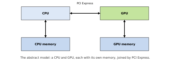
This section will describe a variety of CPU/GPU architectures, with some comments on how a CUDA developer would approach programming the system differently. We describe a variety of CPU configurations, briefly describe integrated GPUs, and finally describe multi-GPU configurations.
We begin with the initial diagram:
Figure 2-1. CPU/GPU Architecture Simplified
An important element of this diagram that was omitted is the “chipset” or “core logic” that connects the CPU to the outside world. Every bit of input and output of the system, from disk and network controllers to keyboards and mice, USB devices and, yes, GPUs, goes through the chipset. Historically, chipsets had been divided into a “south bridge,” which connected most peripherals to the system1, and the “north bridge,” which contained the graphics bus (the Accelerated Graphics Port, until the PCI Express [PCIe] bus displaced it) and a memory controller (“front side bus”) connected to the CPU memory.
Each “lane” in PCI Express 2.0 can theoretically deliver about 500MB/s of bandwidth, and the number of lanes for a given peripheral can be 1, 4, 8, or 16. GPUs require the most bandwidth of any peripheral on the platform, so they generally are designed to be plugged into 16-lane PCIe slots. With packet overhead, the 8GB/s of bandwidth for such a connection delivers about 6GB/s in practice2.
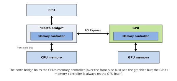
Figure 2-2. CPU/GPU Architecture - North Bridge
Figure 2-2 adds the north bridge and its memory controller to the original simplified diagram.
For completeness, Figure 2-2 also shows the integrated memory controller of the GPU, which is designed under a very different set of constraints than the memory controller of the CPU. The GPU must accommodate so-called isochronous clients, such as video display(s), whose bandwidth requirements are fixed and nonnegotiable. The GPU’s memory controller also is designed with the GPU’s extreme latency-tolerance and vast memory bandwidth requirements in mind. As of this writing, high-end GPUs commonly deliver local GPU memory bandwidths well in excess of 100 GB/s.
GPU memory controllers are always integrated with the GPU, so they are omitted from the rest of the diagrams in this chapter.
Figure 2-3 shows a system with multiple CPUs in a traditional north bridge configuration3. Before multicore processors, applications had to use multiple threads to take full advantage of the additional power of multiple CPUs. The north bridge must ensure that each CPU sees the same coherent view of memory, even though each CPU and the north bridge itself all contain caches.
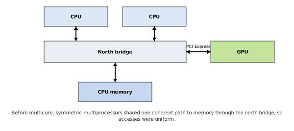
Figure 2-3. Multiple CPUs (SMP Configuration)
Since these so-called “symmetric multiprocessor” (SMP) systems share a common path to CPU memory, memory accesses exhibit relatively uniform performance.
Starting with AMD’s Opteron and Intel’s Nehalem (i7) processors, the memory controller in the north bridge was integrated directly into the CPU, as shown in Figure 2-4. This architectural change improves CPU memory performance.
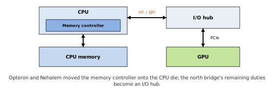
Figure 2-4. CPU with Integrated Memory Controller
For developers, the system of Figure 2-4 is little different than the ones we’ve already discussed. For systems that contain multiple CPUs, as shown in Figure 2-5, things get more interesting.
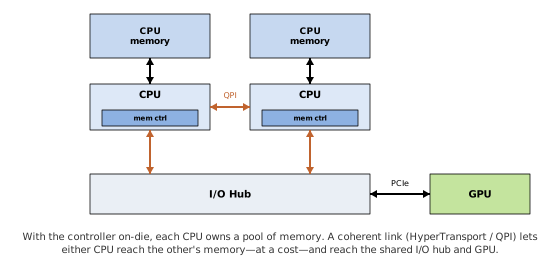
Figure 2-5. Multiple CPUs (NUMA)
For machine configurations with multiple CPUs4, this architecture implies that each CPU gets its own pool of memory bandwidth. At the same time, because multithreaded operating systems and applications rely on the cache coherency enforced by previous CPUs and north bridge configurations, the Opteron and Nehalem architectures also introduced HyperTransport (HT) and QuickPath Interconnect (QPI), respectively.
HT and QPI are point-to-point interconnects that connect CPUs to other CPUs, or CPUs to I/O hubs. On systems that incorporate HT/QPI, any CPU can access any memory location; but accesses are much faster to “local” memory locations whose physical address is in the memory directly attached to the CPU. Nonlocal accesses are resolved by using HT/QPI to snoop the caches of other CPUs, evict any cached copies of the requested data, and deliver the data to the CPU that performed the memory request. In general, the enormous on-chip caches on these CPUs mitigate the cost of these nonlocal memory accesses; the requesting CPU can keep the data in its own cache hierarchy until the memory is requested by another CPU.
To help developers work around these performance pitfalls, Windows Vista and Linux have introduced APIs to enable applications to steer their allocations toward specific CPUs, and to set CPU “thread affinities” so the operating system schedules threads onto CPUs such that most or all of their memory accesses will be local.
A determined programmer can use these APIs to write contrived code that exposes the performance vulnerabilities of NUMA, but the more common (and insidious!) symptom is a slowdown due to “false sharing” where two threads running on different CPUs cause a plethora of HT/QPI transactions by accessing memory locations that are in the same cache line. So NUMA APIs must be used with caution: although they give programmers the tools to mitigate NUMA performance problems, they also can make it easy for developers to inflict them on themselves.
One approach to mitigating the performance impact of nonlocal memory accesses is to enable memory interleaving, in which physical memory is evenly split between all CPUs on cache line boundaries5. For CUDA, this approach works well on systems that are designed exactly as shown in Figure 2-5, with multiple CPUs in a NUMA configuration connected by a shared I/O hub to the GPU(s). Since PCI Express bandwidth is often a bottleneck to overall application performance, however, many systems have separate I/O hubs to service more than one PCI Express bus, as shown in Figure 2-6.
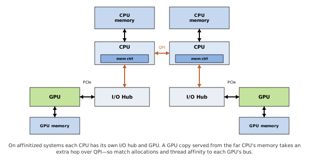
Figure 2-6. Multi-CPU (NUMA Configuration), Multiple Buses
In order to run well on such “affinitized” systems, CUDA applications must take care to use NUMA APIs to match memory allocations and thread affinities to the PCI Express bus attached to a given GPU. Otherwise, memory copies initiated by the GPU(s) are nonlocal and the memory transactions take an extra “hop” over the HT/QPI bus. Since GPUs demand a huge amount of bandwidth, these DMA operations greatly reduce the ability of HT/QPI to serve its primary purpose. Compared to false sharing, the performance impact of nonlocal GPU memory copies is a much more plausible performance risk for CUDA applications.
Intel’s Sandy Bridge class processors take another step toward full system integration, by integrating the I/O hub into the CPU. A single Sandy Bridge CPU has up to 40 lanes of PCI Express bandwidth (remember that one GPU can use up to 16 lanes, so 40 is enough for more than 2 full-size GPUs).
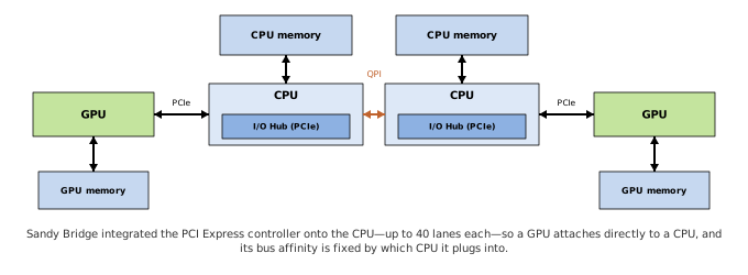
Figure 2-7. Multi-CPU with integrated PCI Express
For CUDA developers, PCI Express integration brings bad news and good news.
The bad news is that PCI Express traffic is always affinitized: designers cannot build systems like the system of Figure 2-5, in which a single I/O hub serves multiple CPUs; all multi-CPU systems resemble Figure 2-7. As a result, GPUs associated with different CPUs cannot perform peer-to-peer operations.
The good news is that the CPU cache can participate in PCI Express bus traffic: the CPU can service DMA read requests out of cache, and writes by the GPU are posted to the CPU cache.
The integration that produced Figure 2-7 did not stop at the CPU. The most consequential recent trend in system design is the packaging of the CPU and GPU—or of many GPU dies—into a single module or tightly coupled pair, joined not by a general-purpose bus but by a coherent, high-bandwidth interconnect. Two techniques make it possible. Chiplet designs break what was once a single large die into several smaller ones, improving yield and letting a vendor mix process nodes; advanced packaging—silicon interposers (2.5D), 3D die stacking, and dense organic substrates—then reconnects those dies with far more bandwidth than a circuit-board trace could carry. The links themselves are proprietary and coherent: NVIDIA’s NVLink (and its chip-to-chip variant, NVLink-C2C) and AMD’s Infinity Fabric.
AMD’s Instinct accelerators show the range. The MI250X places two GPU dies on one module, joined by Infinity Fabric and backed by 128 GB of HBM2e; software still sees two GPUs. The MI300X goes further, stacking eight CDNA 3 GPU chiplets over I/O dies on an interposer, with 192 GB of HBM3 and 5.3 TB/s of bandwidth, presented as one enormous GPU (Figure 2-8). And the MI300A dissolves the CPU/GPU boundary outright: an APU that puts Zen 4 CPU chiplets and CDNA 3 GPU chiplets on one package, sharing 128 GB of HBM3 in a single coherent address space—no host-to-device copy required. (The MI250X powers the Frontier supercomputer; the MI300A, El Capitan.)
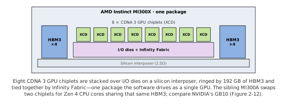
Figure 2-8. AMD Instinct MI300X: a chiplet GPU package.
NVIDIA’s counterpart is the Grace Hopper superchip, which joins a Grace Arm CPU and a Hopper GPU over coherent NVLink-C2C at 900 GB/s—the CPU’s LPDDR5X and the GPU’s HBM remaining distinct memories, but coherent (Section 2.4). Its derivatives scale in both directions: GB200 pairs a Grace CPU with two Blackwell GPUs as the building block of the NVL72 rack (Section 2.3), while the GB10 brings the same idea to the desktop with a single, physically unified memory pool (Section 2.2). For the CUDA programmer, the trajectory is clear: the discrete CPU-plus-GPU-over-PCIe model of the opening figures is giving way to systems where the two are, increasingly, one—and the interconnects that bind them are the subject of Section 2.7.
For simplicity, the south bridge is omitted from all diagrams in this section.↩︎
PCI 3.0 uses a more sophisticated mechanism for error detection that incurs much less overhead.↩︎
For reasons that will soon become clear, we offer this diagram more for historical reference than because there are CUDA-capable computers with this configuration.↩︎
On such systems, the CPUs also may be referred to as “nodes” or “sockets.”↩︎
A cynic would say that this makes all memory accesses “equally bad.”↩︎